
Objectives
Based on the current level of knowledge and flowing the proposed concepts for normally-off GaN MOS-HEMT, following main objectives of the proposed project are targeted:
- Gaining a fundamental understanding of the origin and formation of SD in III-N heterostructures;
- Analysis of technological SD control allowing their suppression below 1.8 x 1013 cm-2 at oxide/III-N interfaces;
- Development of highly safe normally-off GaN MOS-HEMTs based on SD engineering concept, with adjustable positive Vth above +2 V without compromising output current capability;
- Analysis and development of alternative highly safe normally-off MOS-HEMTs based on polarization charge engineering concept, also with freely adjustable positive Vth and uncompromised output current capability;
- Thorough analysis of conceptual reliability issues in the developed normally-off MOS-HEMTs, in particular Vth bias and temperature instability and gate oxide integrity, that will facilitate development of safe and reliable GaN switching device;
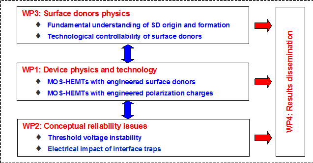
The working activities will be broken down into four self-containing work packages. The work packages (WPs) represent three basic research areas and interactions between them, necessary for a new solid-state device concept development. Principles of SD formation and possibilities for Nds technological control will be studied in WP3 led by SUT IP. The gained knowledge will be directly exploited for devices design and technology development in WP1 (lead by IEE SAS), within close interaction between WP1 and WP3. In WP2, led by HU RCIQE, the fabricated devices will be thoroughly analyzed so that the basic conceptual (i.e. those related to MOS-HEMT gate structure) reliability issues will be analyzed and addressed via technology optimization ensured by the close interaction between WP1 and WP2. All the results achieved in particular WP will be disseminated via publications in the high-quality scientific journals and presentations in the reference international conferences focused on GaN based electron devices research and applications. Dissemination activities of WP4 (coordinated by MFA) will be addressed also in the public web page to spread the information on activities of the consortia towards scientific community.
Interactions between the project partners will provided by regular skype conferences, or on basis of mutual interactions. Annual meetings will be held either in Slovakia or in Japan. The project will be coordinated by IEE SAS.